The Progression of Semiconductor Manufacturing Techniques
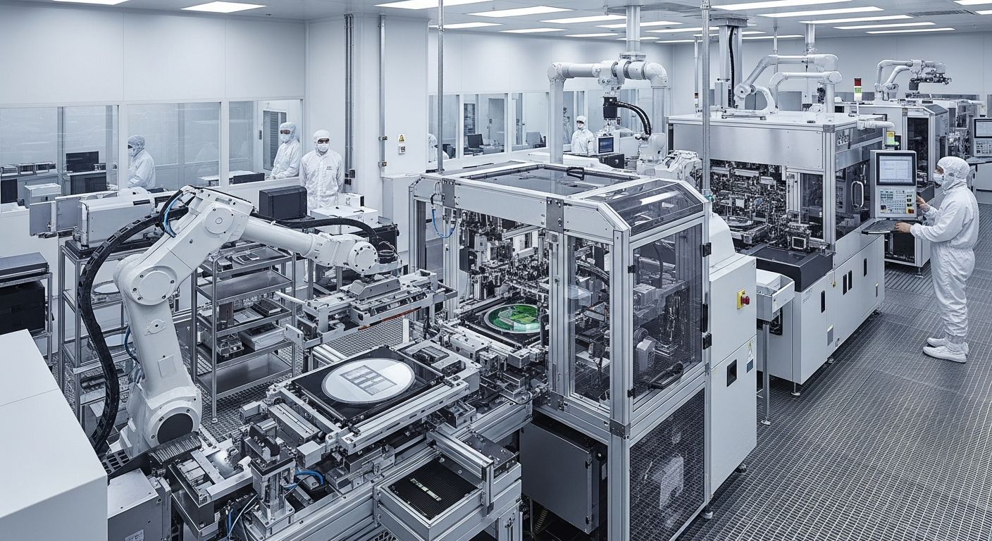
Semiconductor manufacturing techniques have undergone a profound evolution, transforming from rudimentary processes to highly sophisticated methodologies. This progression is fundamental to the advancements seen across all sectors of modern technology, enabling the creation of smaller, faster, and more energy-efficient electronic components. Understanding this journey reveals the intricate engineering and scientific breakthroughs that underpin our digital world, from personal computing devices to complex networking infrastructure and advanced processors.

Early Developments in Semiconductor Manufacturing
The journey of semiconductor manufacturing began with foundational discoveries in material science, particularly with silicon and germanium. Early techniques focused on creating single-crystal ingots and then slicing them into wafers. The initial fabrication processes involved basic doping methods and photolithography to define circuit patterns. These early steps, while primitive by today’s standards, laid the groundwork for all subsequent innovations in electronics. The ability to precisely control the electrical properties of materials was a monumental leap, enabling the transition from vacuum tubes to solid-state components, which drastically reduced the size and power consumption of early computing systems.
Miniaturization and Advanced Lithography in Computing
The relentless drive for miniaturization has been a defining characteristic of semiconductor innovation. As the demand for more powerful processors and digital hardware grew, so did the need to pack more transistors onto a single chip. This led to significant advancements in lithography, the process of transferring circuit patterns onto a wafer. From visible light, manufacturers transitioned to ultraviolet (UV) light, and then to deep ultraviolet (DUV) and extreme ultraviolet (EUV) lithography. Each technological leap allowed for the creation of ever-smaller features, pushing the boundaries of what was thought possible in computing and enabling the exponential growth in processing power that has defined the modern era of technology.
Materials Science and Device Architecture for Modern Electronics
The evolution of semiconductor manufacturing is not solely about shrinking features; it also involves radical changes in materials science and device architecture. Early transistors were planar, but as dimensions shrunk, leakage currents and performance limitations became significant challenges. This led to the development of new transistor structures, such as FinFETs (Fin Field-Effect Transistors), which allowed for better control over the current flow and improved power efficiency. Concurrently, the introduction of new materials, like high-k dielectrics to replace silicon dioxide in gate insulators, helped manage leakage and further enhance performance in various devices and gadgets, impacting everything from displays to mobile systems.
The Role of Advanced Packaging and Integration
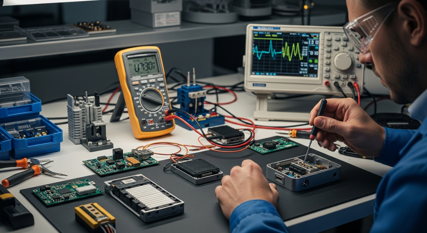
Beyond the wafer fabrication process, advanced packaging and integration techniques have become critical for enhancing the performance and functionality of semiconductor components. Traditional packaging simply protected the chip, but modern approaches involve sophisticated 3D stacking, system-in-package (SiP), and chiplet designs. These methods allow for the integration of diverse components, such as processors, memory (storage), and specialized accelerators, into a single, compact unit. This not only improves data transfer speeds and reduces power consumption but also enables the creation of highly complex systems for networking and other applications, pushing the boundaries of what integrated circuits can achieve.
Future Directions in Semiconductor Technology
The future of semiconductor manufacturing promises continued innovation, driven by the increasing demands of artificial intelligence, quantum computing, and advanced digital systems. Research is actively exploring novel materials beyond silicon, such as gallium nitride (GaN) and silicon carbide (SiC) for power electronics, and 2D materials like graphene for next-generation devices. Furthermore, new manufacturing paradigms, including atomic layer deposition and advanced metrology, are being developed to achieve even greater precision. These ongoing developments are crucial for powering the next wave of technological breakthroughs, from more intelligent gadgets to entirely new computing architectures and robust components.
Semiconductor manufacturing has progressed from a nascent field to a highly sophisticated global industry, continually pushing the boundaries of physics and engineering. The journey has been characterized by a relentless pursuit of miniaturization, the introduction of advanced materials, and innovative architectural designs. This continuous evolution underpins virtually every piece of modern electronics, from the smallest sensors to the most powerful supercomputers, demonstrating the enduring impact of these complex manufacturing techniques on our interconnected world.


